[Poster] SFU Physics Poster Competition 2023
Abstract
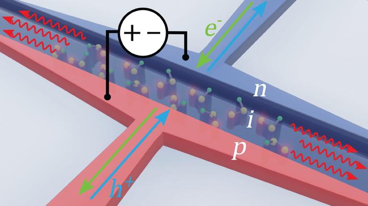
The T-centre defect in silicon is a competitive spin-photon interface for quantum computing and communication applications. In addition to its properties as a qubit, it also has potential as an on-chip light source by electrical injection, operating in silicon. To fully realize this property, electro-optical devices must be designed and optimized for the task. These devices must also couple light to waveguides for integration with other silicon photonic devices. Isolating single T centres in these devices could also allow for on-chip single photon sources. This work explores aspects of this design optimization and outlines the plan for evaluation. This electrical interface is another step towards integration of the T centre in large-scale quantum photonic circuits on a single chip for high-performance quantum technologies.
Michael Dobinson
PhD Candidate
Research interests include quantum computing, optics, photonics, and microelectronics.